


SKU:WSAL6979
OpenEP4CE10-C Standard, ALTERA Development Board
Abholverfügbarkeit konnte nicht geladen werden
Overview
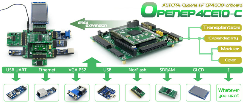
OpenEP4CE10-C is an FPGA development board that consists of the mother board DVK600 and the FPGA core board CoreEP4CE10.
OpenEP4CE10-C supports further expansion with various optional accessory boards for specific application. The modular and open design makes it the ideal for starting application development with ALTERA Cyclone IV series FPGA devices. OpenEP4CE10-C enables you to start your design with the Nios II processor easily and quickly.
What's on the mother board
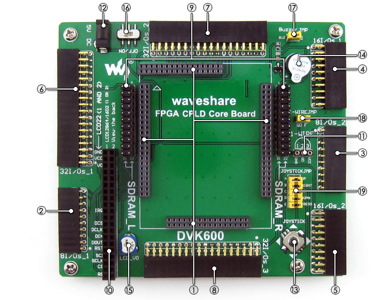
- FPGA CPLD core board connector: for easily connecting core boards which integrate an FPGA CPLD chip onboard
- 8I/Os_1 interface, for connecting accessory boards/modules
- 8I/Os_2 interface, for connecting accessory boards/modules
- 16I/Os_1 interface, for connecting accessory boards/modules
- 16I/Os_2 interface, for connecting accessory boards/modules
- 32I/Os_1 interface, for connecting accessory boards/modules
- 32I/Os_2 interface, for connecting accessory boards/modules
- 32I/Os_3 interface, for connecting accessory boards/modules
All the I/O interfaces above:
- capable of being simulated as USART, I2C, SPI, PS/2, etc.
- capable of driving devices such as FRAM, FLASH, USB, Ethernet, etc.
- SDRAM interface
- for connecting SDRAM accessory board
- also works as FPGA CPLD pins expansion connectors
- LCD interface, for connecting LCD22, LCD12864, LCD1602
- ONE-WIRE interface: easily connects to ONE-WIRE devices (TO-92 package), such as temperature sensor (DS18B20), electronic registration number (DS2401), etc.
- 5V DC jack
- Joystick: five positions
- Buzzer
- Potentiometer: for LCD22 backlight adjustment, or LCD12864, LCD1602 contrast adjustment
- Power switch
- Buzzer jumper
- ONE-WIRE jumper
- Joystick jumper
For jumpers 17-19:
- short the jumper to connect to I/Os used in example code
- open the jumper to connect to other custom pins via jumper wires
The DVK600 supports a wide range of different core boards, therefore, some of the interfaces may be Not-Connected and useless while connecting to certain core board. For instance, while connecting to Core3S500E/CoreEP2C8, the '⑧ 32I/Os_3' is Not-Connected.
What's on the CoreEP4CE10
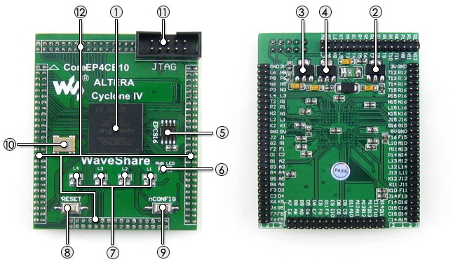
- EP4CE10F17C8N:the ALTERA Cyclone IV FPGA device which features:
- Operating Frequency:50MHz
- Operating Voltage:1.15V~3.465V
- Package:BGA256
- I/Os:164
- LEs:10K
- RAM:414kb
- PLLs:2
- Debugging/Programming: supports JTAG
- AMS1117-3.3 (on bottom side), 3.3V voltage regulator
- AMS1117-2.5 (on bottom side), 2.5V voltage regulator
- AMS1117-1.2 (on bottom side), 1.2V voltage regulator
- EPCS16, onboard serial FLASH memory, for storing code
- Power indicator
- LEDs
- Reset button
- nCONFIG button: for re-configuring the FPGA chip, the equivalent of power reseting
- 50M active crystal
- JTAG interface: for debugging/programming
- FPGA pins expander, VCC, GND and all the I/O ports are accessible on expansion connectors for further expansion
Photos
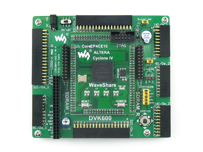 OpenEP4CE10-C Development Board
 OpenEP4CE10-C Development Board
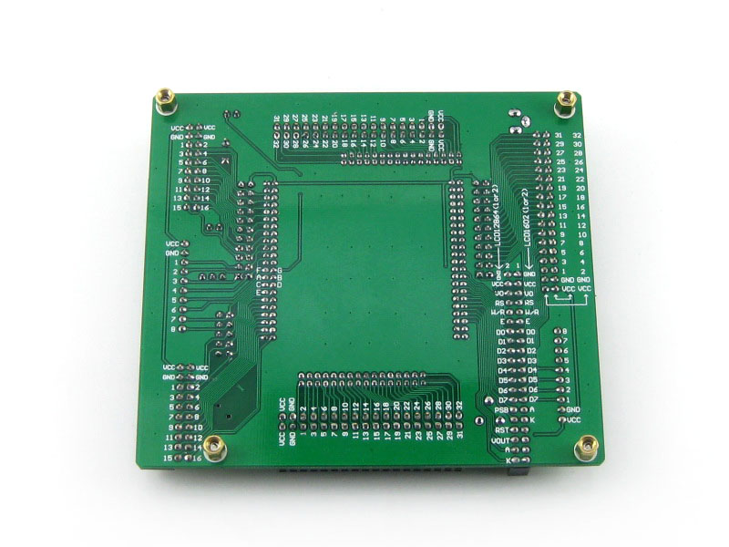 OpenEP4CE10-C Development Board back view
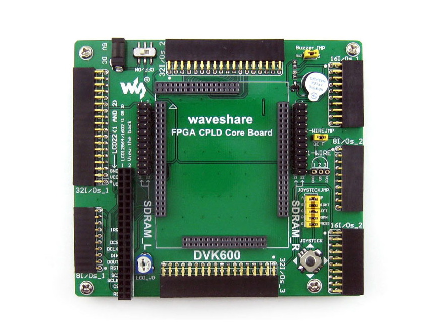 Mother Board DVK600
 FPGA core board CoreEP4CE10
 FPGA core board CoreEP4CE10
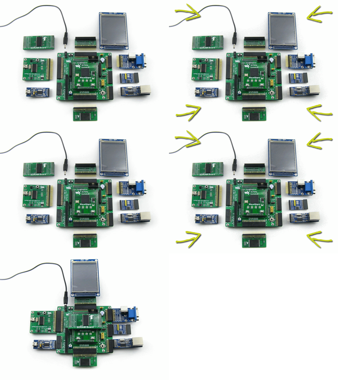 Connecting to various peripherals
 Connecting to 3.2inch Touch LCD
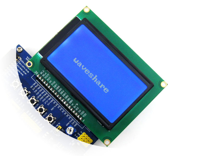 Connecting to LCD12864
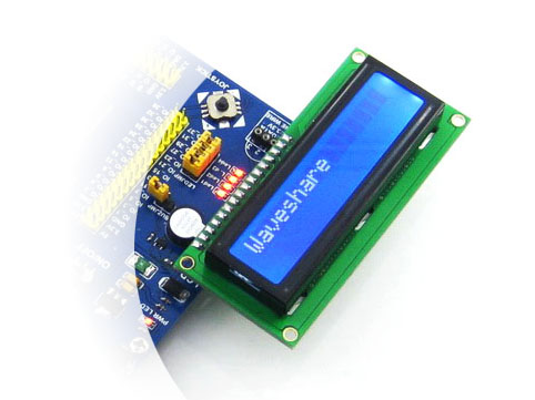 Connecting to LCD1602
 Connecting to RS232 Board
 Connecting to RS485 Board
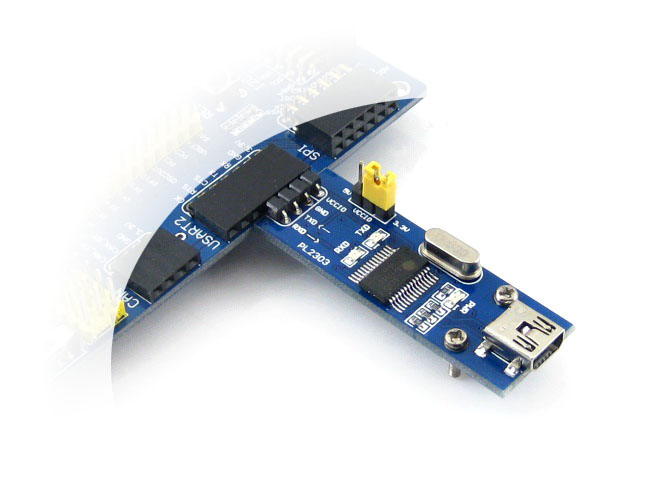 Connecting to USB UART Board
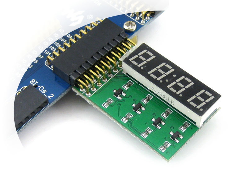 Connecting to 8 SEG LED Board
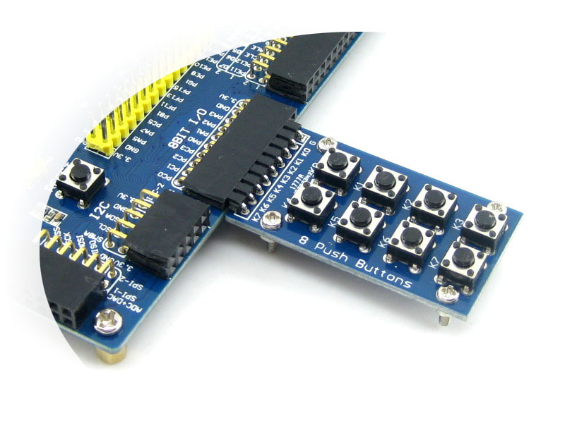 Connecting to 8 Push Buttons
 Connecting to 5 IO Keypad
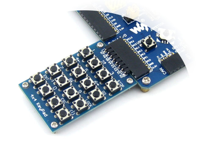 Connecting to 4x4 Keypad
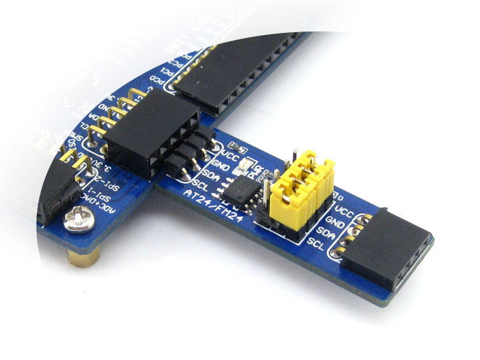 Connecting to EEPROM Board
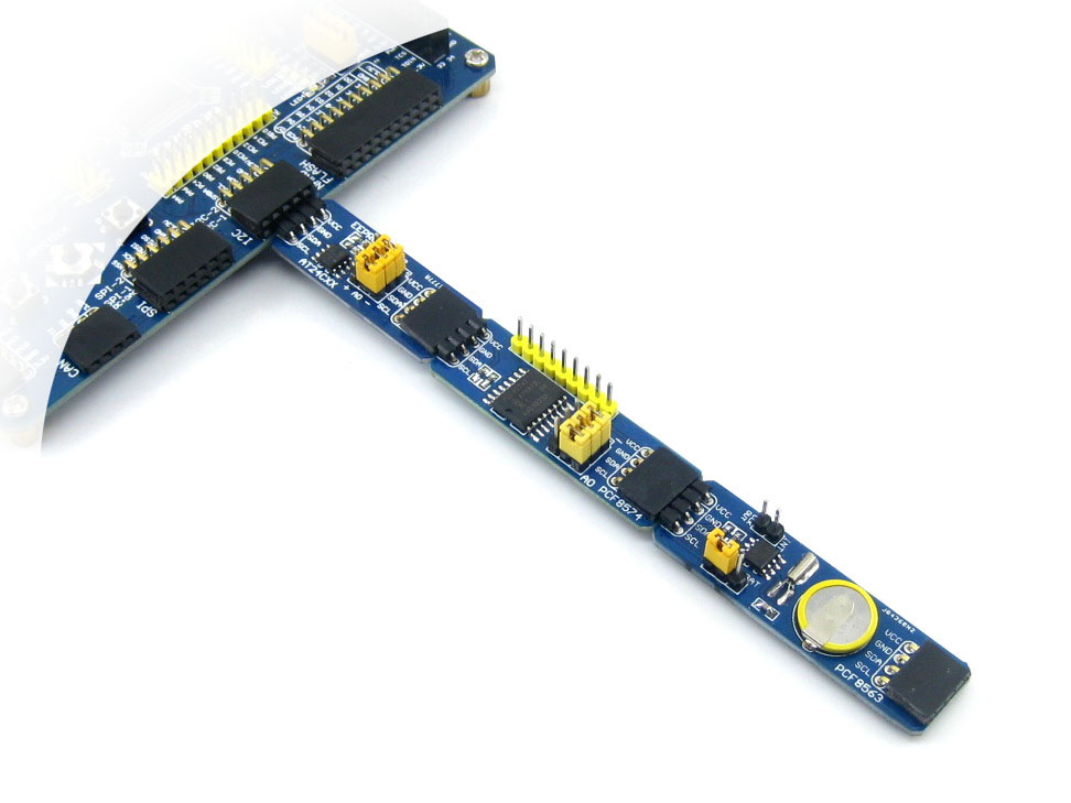 Multi peripherals connected to one interface
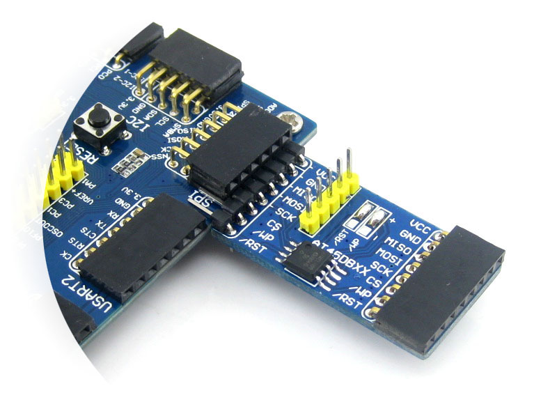 Connecting to DataFlash Board
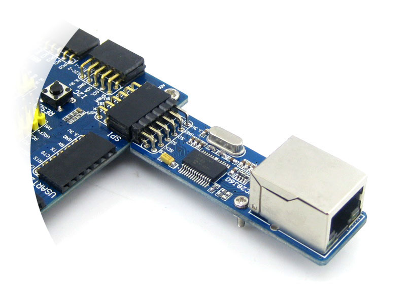 Connecting to Ethernet Board
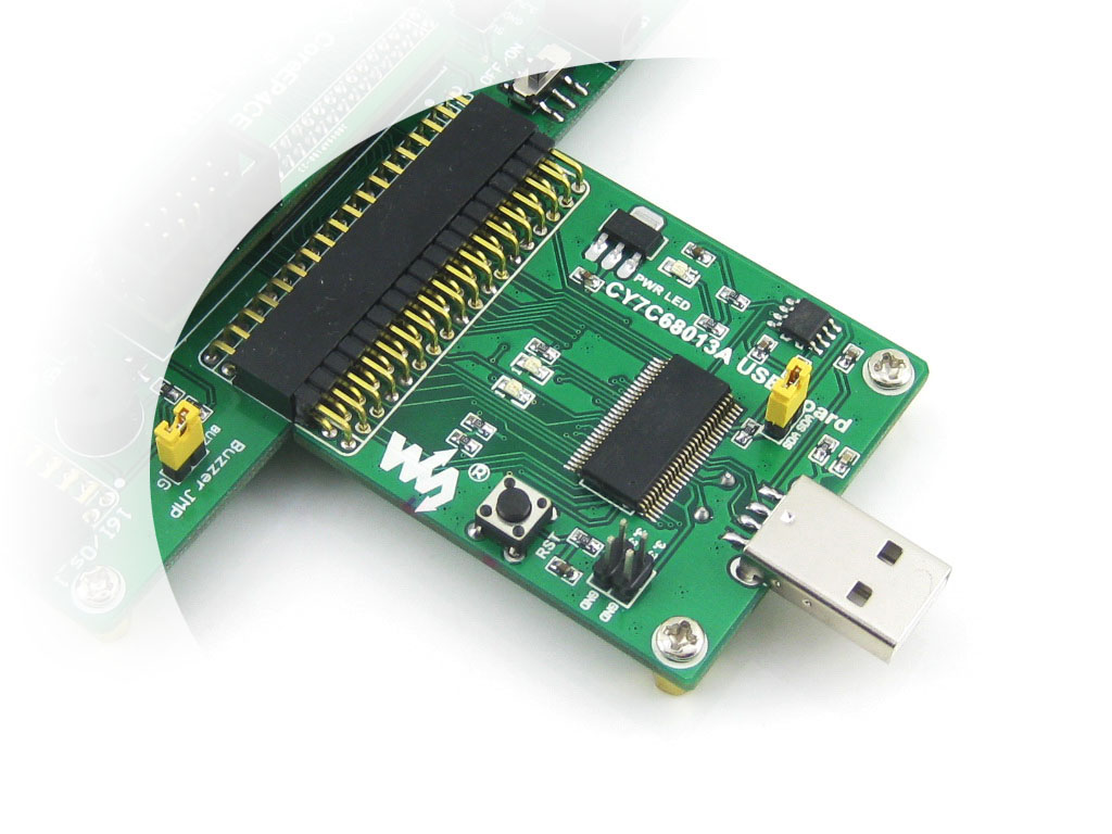 Connecting to CY7C68013A USB Board
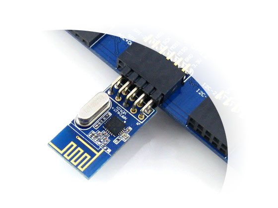 Connecting to NRF24L01 RF Board
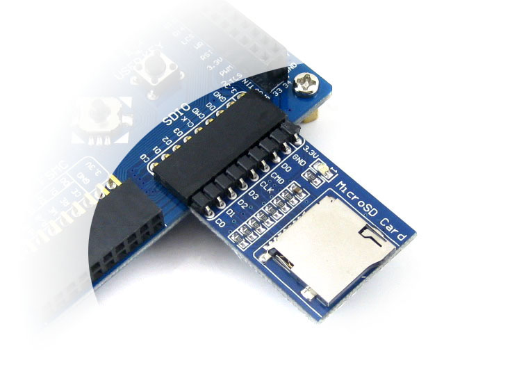 Connecting to Micro SD Storage Board
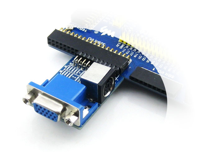 Connecting to VGA PS2 Board
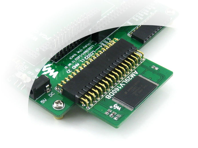 Connecting to SDRAM Board
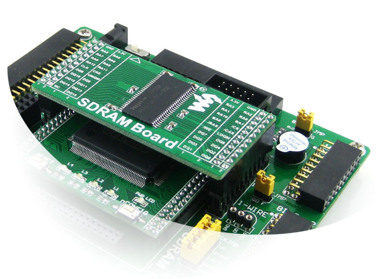 Connecting to SDRAM Board
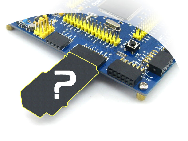 Connecting to any accessory board you need
Note: The OpenEP4CE10-C does NOT integrate any programming/debugging function, a programmer/debugger is required.
Examples
The OpenEP4CE10-C FPGA development board comes with various examples codes for the supported peripherals, which give you a quick start to develop your own application.
| Peripheral | Description | Interface | Verilog | VHDL | NIOS II C |
|---|---|---|---|---|---|
| S29GL128P | NorFLASH | 32I/Os | Y | ||
| AT24CXX | EEPROM | I2C | √ | √ | √ |
| FM24CXX | FRAM | I2C | √ | √ | √ |
| AT45DBXX | DATAFLASH | SPI | √ | ||
| SD card | FLASH | SPI | √ | ||
| H57V1262GTR | SDRAM | parallel | √ | ||
| PCF8563 | RTC | I2C | √ | ||
| DS18B20 | Temperature sensor | 1-WIRE | √ | √ | √ |
| SP3232 | Serial communication | UART | √ | √ | √ |
| SP3485 | Serial communication | UART | √ | √ | √ |
| PL2303 | USB TO UART | UART | √ | √ | √ |
| FT245 | USB TO FIFO | parallel | √ | ||
| CY7C68013A | USB DEVICE | I/Os | √ | ||
| ENC28J60 | Ethernet controller | SPI | √ | ||
| Buzzer | Sound device | 1I/O (PWM) | √ | √ | √ |
| PS/2 keyboard | Input device | PS/2 | √ | √ | |
| Single buttons | Input device | ---- | √ | √ | √ |
| 4x4 keypad | Input device | 8I/Os | √ | √ | √ |
| Joystick | Input device | 5I/Os | √ | √ | √ |
| LED | Display device | ---- | √ | √ | √ |
| 8 SEG LED | Display device | 13I/Os | √ | √ | √ |
| VGA monitor | Display device | VGA | √ | √ | |
| Character LCD | Display device | 11I/Os | √ | √ | |
| Graphic LCD | Display device | 11I/Os | √ | ||
| 3.2 inch multi-color LCD + touch screen | Display device + Input device | 32I/Os | √ |
Debugging/Programming Interface
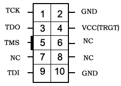
The OpenEP4CE10-C FPGA development board integrates JTAG interface for programming/debugging.
JTAG Signal Names & Description
| Pin | Signal Name | Description |
|---|---|---|
| 1 | TCK | Clock signal |
| 2 | GND | Signal ground |
| 3 | TDO | Data from device |
| 4 | VCC(TRGT) | Target power supply |
| 5 | TMS | JTAG state machine control |
| 6 | NC | No connect |
| 7 | NC | No connect |
| 8 | NC | No connect |
| 9 | TDI | Data to device |
| 10 | GND | Signal ground |
JTAG Header Pinout
Development Resources
- Related Software (Quaters II, NIOS II etc.)
- Demo Code (Verilog, VHDL and NIOS II C)
- Schematic (PDF)
- FPGA Development Documentations (Datasheets etc.)
Wiki:www.waveshare.com/wiki/OpenEP4CE10-C
Lieferumfang
- OpenEP4CE10-C development board x 1
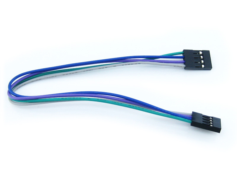
- 4-pin wire x 2
- 2-pin wire x 2
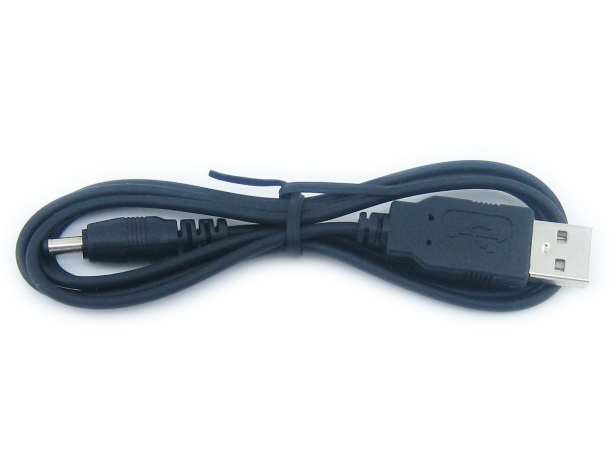
- USB power cable x 1

Zahlungsmethoden
Zahlungsmethoden
